
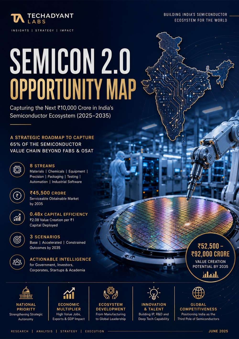
India funds the fab; the value is elsewhere
In July 2026 the Union Cabinet approved the second phase of the India Semiconductor Mission — a roughly ₹1.27 lakh crore, six-pillar programme that, for the first time, extends state support beyond fabrication into materials, equipment, chemicals and the wider component ecosystem. That decision reframes the Indian semiconductor story. The fab is no longer the whole ambition; it is the anchor. And the fab is only about 35% of the semiconductor value chain. The other 65% — materials, chemicals, equipment, precision manufacturing, packaging, testing, automation and industrial software — is where roughly 78% of the industry's gross-margin pool actually sits, and it is the part India has barely started to fund. This report maps that 65%.
What Semicon 2.0 is
Techadyant Labs defines Semicon 2.0 as the deliberate, coordinated build-out of the eight-stream semiconductor ecosystem beyond fab and OSAT. Semicon 1.0 — the ₹76,000 crore first phase launched in December 2021 — did the necessary anchor work: Tata Electronics' Dholera fab, Micron's Sanand facility, and the first wave of assembly and packaging commitments moved India from the periphery of the global map to a credible manufacturing geography. Semicon 2.0 is the ecosystem that decides whether those anchors compound into an industry, or quietly keep importing everything upstream. The distinction matters because value, margin and strategic vulnerability all sit upstream of the fab, not inside it.
The prize: a Rs 95,500 crore opportunity
The ten-year cumulative addressable opportunity across the eight streams is modelled at about ₹427,500 crore in geographic terms (TAM), of which India's serviceable available market (SAM) is ₹217,600 crore and the realistically obtainable market (SOM) is about ₹95,500 crore by 2035 — larger than the combined market capitalisation of India's listed semiconductor-ecosystem companies today. These are Techadyant Labs' own modelled estimates, presented across Base, Accelerated and Constrained scenarios; they should be read as directional sizing of the opportunity, not as forecasts. The point is not the decimal place. It is that a serviceable market of this scale exists in the layer of the industry that currently receives the least private capital and the least policy attention.
The eight streams, ranked
The opportunity is unevenly distributed. Equipment (about ₹9,580 crore a year by 2035) and Packaging (about ₹9,160 crore) are the largest pools; Industrial Software (about ₹4,830 crore) is India's most asymmetric play, because the country's existing IT and engineering base can be repurposed for manufacturing execution systems, digital twins and yield-optimisation software with marginal incremental capital. Chemicals, Materials and Testing are critical enablers requiring targeted capital; Precision Manufacturing and Automation are higher-uncertainty but high-leverage. The strategic error would be to treat the eight as a single undifferentiated “ecosystem” opportunity — the returns, time horizons and capital intensity differ by an order of magnitude across them.
How import-dependent India still is
The reason this matters now is exposure. India imports an estimated 99% of its lithography equipment, 95% of its photoresists, 92% of its specialty gases and 88% of its metrology tools. The fab can be built in Dholera; the chain that feeds it is still abroad. Of the ₹76,000 crore Semicon 1.0 outlay, only a small fraction was explicitly directed at specialty materials and equipment — which is precisely the gap Semicon 2.0's “machines and materials” pillar now begins to address. Every one of these dependencies is simultaneously a vulnerability and an addressable opportunity surface.
The single scariest chokepoint
The concentration risk is starkest in photoresist. A handful of Japanese firms control the overwhelming majority of global photoresist supply — on the most recent data, roughly 87–91%, rising toward 91% for the advanced extreme-ultraviolet grades that leading-edge fabs depend on. India's domestic photoresist capability is effectively zero. A single supply shock in this one input would reprice the entire national ambition. A strategic joint venture with a Korean or European player to establish India-based photoresist manufacturing is, on the report's analysis, the highest-leverage single intervention in the materials domain.
Three tiers, three time horizons
The eight streams resolve into three capital-allocation tiers. Tier 1 (Speed up) — Industrial Software, Packaging, Testing and Automation — are immediate deployments with one-to-three-year time-to-revenue and the highest internal rates of return. Tier 2 (Invest now) — specialty gases, precision components, CMP slurries and sputtering targets — are three-to-five-year horizons that need government co-investment. Tier 3 (Long horizon) — a photoresist JV, wafer manufacturing, metrology tools and sub-14nm lithography — require sovereign commitment and strategic partnerships over five to ten years. The tiering is the actionable core of the report: it converts a map of opportunity into a sequence of decisions.
The window is open now
The window for capturing this opportunity is finite. Geopolitical realignment has opened a period — perhaps five to seven years — in which Western capital, technology and strategic intent are aligned with Indian capability building. India's engineering-talent dividend peaks around 2032, and global semiconductor overcapacity could emerge by the mid-2030s. Action deferred to 2030 is likely to meet a closed opportunity landscape. Semicon 1.0 built the fabs; Semicon 2.0 decides who captures the value they create.
What the full report adds
The full ~180-page edition carries all fifteen chapters: a stream-by-stream deep dive for each of the eight opportunity surfaces (market size, import dependency, competitive structure, India's position and the specific plays), the complete TAM/SAM/SOM model across three scenarios, the OSAT cost-arbitrage analysis, the talent-pipeline and finishing-school proposal, a state-by-state comparison, the risk register and ten-year roadmap, and the investment thesis with the three-tier allocation framework. Twenty-six figures and a ten-sheet data workbook throughout, with all market-sizing labelled as Techadyant Labs' own modelling and load-bearing external facts traced to source.
Unlock the complete report
You’re reading the free preview. The full analysis continues with six more sections and the downloadable PDF edition.
- 🔒04 · Water, power & land
- 🔒05 · The packaging layer
- 🔒06 · Who captures the value
- 🔒07 · The talent constraint
- 🔒08 · Second-order effects
- 🔒09 · What to watch · references
You’ll be asked to sign in, then complete a one-time secure purchase.